)
Experiment No. (6
Decoder Circuit
Objective:
Understanding the construction and operating principles of decoder circuits.
:
Introduction
A decoder is a logic circuit that will detect the presence of a specific binary
number . The input to the decoder is a parallel binary number and the output is a
binary signal that indicates the presence or absence of that specific number.
The AND gate can be used as a basic decoder
will be a binary 1 only when all inputs are binary 1. Proper connections of AND
:
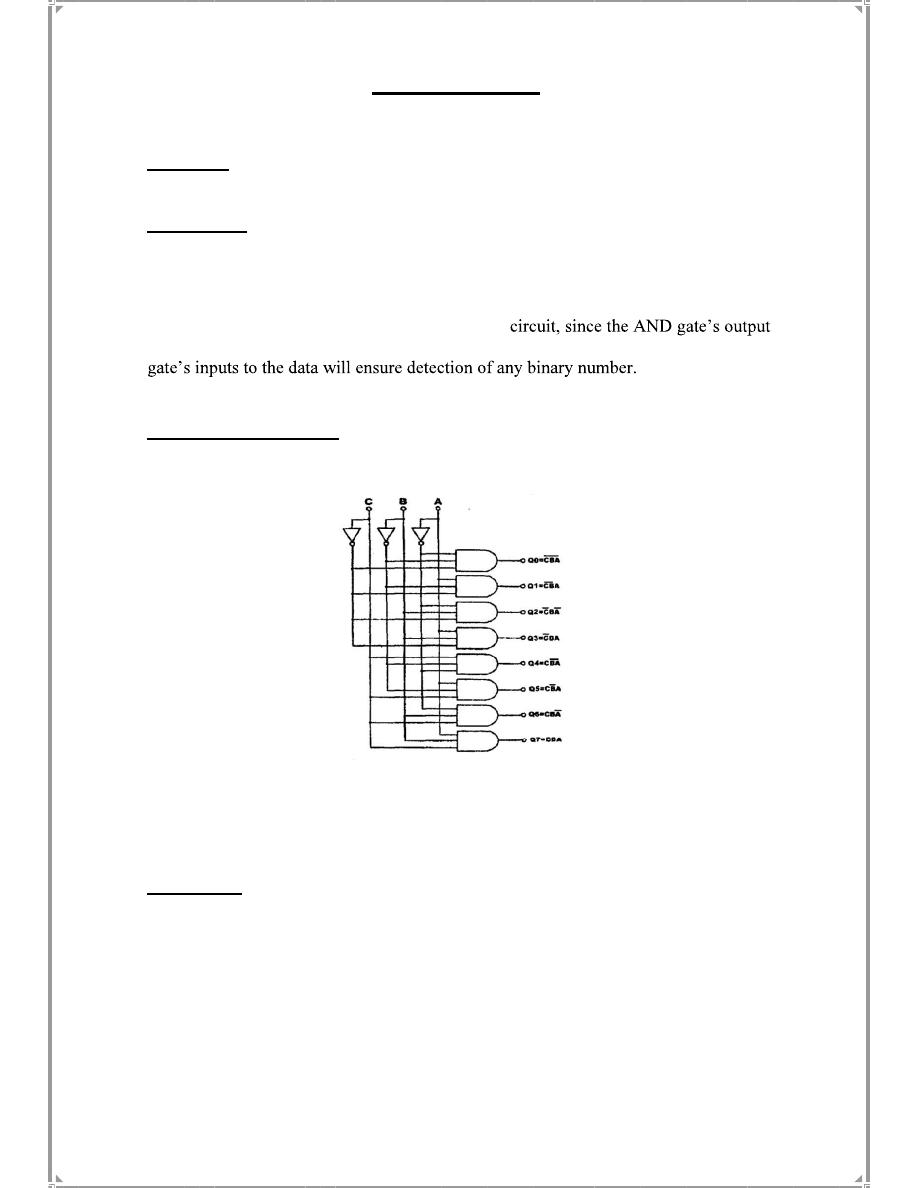
Octal Decoder
-
to
-
Binary
A
binary-to-octal
decoder
is
shown
in
Fig.(6-1).
There
are
3
binary
inputs
A,B,C
and
octal
outputs
Q
0
-Q
7
.
If
CBA="010"
output
Q
2
='1'.
When
CBA="111"
output
Q
7
=1
Equipments Required:KL-31001 Digital Logic Lab; Module KL-33004/KL-33005.
Procedures:
(a) Constructing a 2-to-4 Decoder with Basic Gates.
1. Block
C
of module KL-33005 will be used in this section of the experiment.
Connect Vcc to +5V.
Fig. (6 - 1)
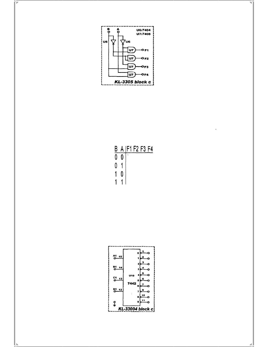
to
4
F
1
&
outputs F
. Connect
and SW0
2.Connect inputs
B
, A to Data Switches SW1
respectively.
L
-
Logic Indicators L
3. Follow the input sequences for A and B in Table (6-1) and record output states
(b) Constructing a BCD to Decimal Decoder with TTL IC.
33004 will be used in this section of the
-
(7442) on block c of module KL
10
1. U
experiment. 7442 is a BCD-to-Decimal decoder IC.
Fig. (6-2)
Table (6-1)
Fig. (6-3)
3
0
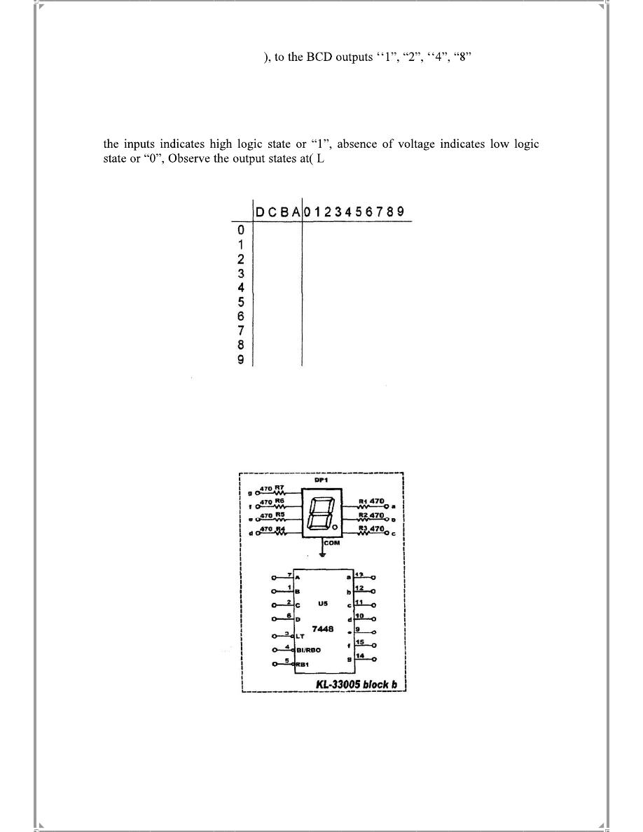
2. Connect inputs( A
l
, B
l
, C
l
, D
l
of one of the
Thumb wheel Switches respectively. Connect outputs (0-9) to Logic Indicator (L9- L0).
The thumb wheel switch is a mechanical device that converts numbers to BCD codes.
3. Adjust the Thumb wheel Switches according to Table (6-2), Presence of voltage at
0
-L
9
). Record input and output logic states
in table (8-2)
(c) BCD - to -7-Segment Decoder.
1.Connect inputs D, C, B, A of U
5
(7448) on block b of module KL-33005 to Data
Switches SW
3
, SW
2
, SW
1
,
SW
0
respectively. The 7448 is a BCD-to-7 segment
Table (6-2)
Fig. (6-4)
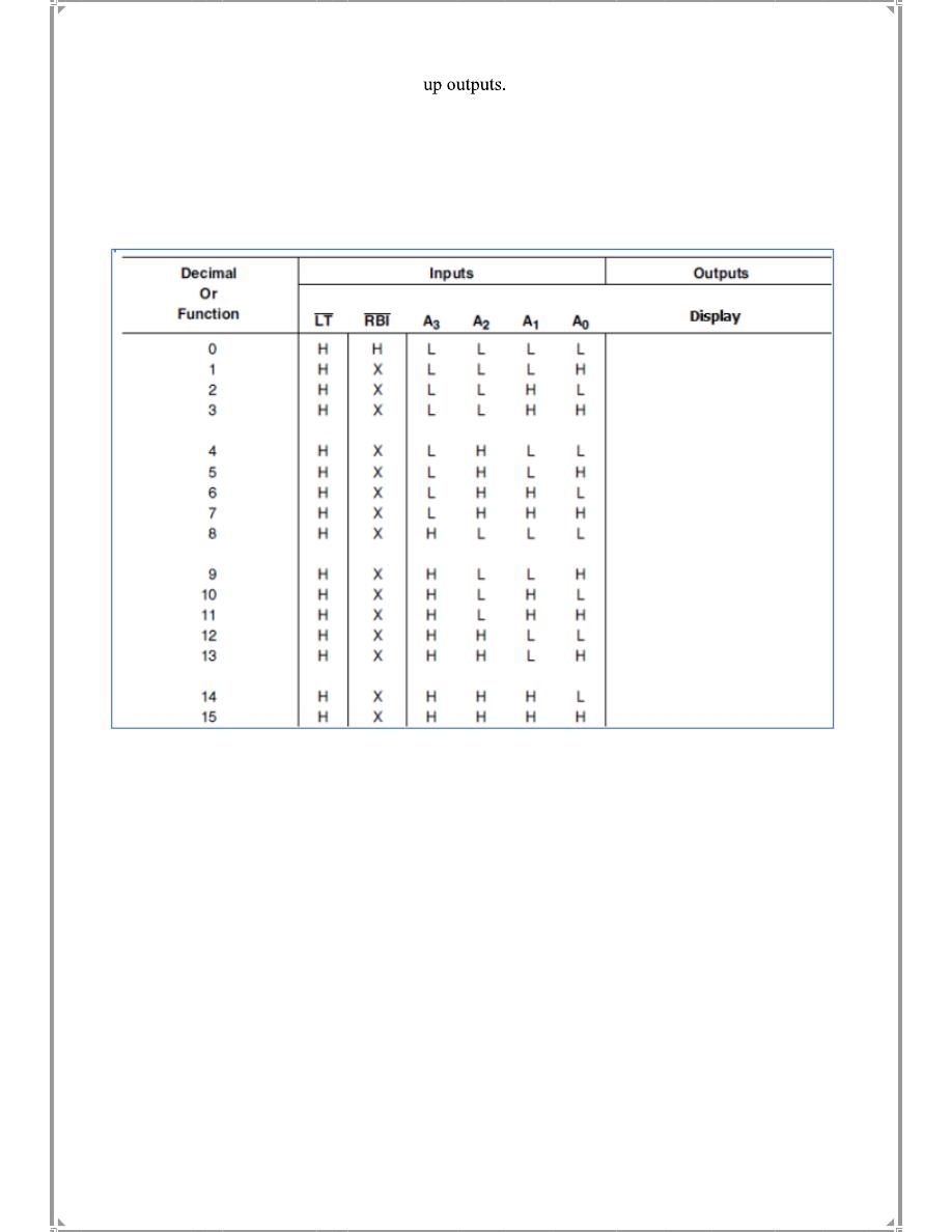
decoder/driver with internal pull-
3. Follow the input sequences
for
D,
C,
B,
A
in
table
(6-3)
and
record
outputs
of
the
7-
segment
display.
Table(6-3)
2
. Connect LT
to DIP Switch 1.0, BI
to DIP 1.1 and RBI to to DIP 1.2.
4. Set
BI
to
Low
while
LT & RBI
remains
High.
Repeat
step
3.
Are
the
outputs
any different from step 3.
5. Set
LT to Low
and
RBI & BI
to
High.
Repeat
step
3.
Are
the
outputs
any
different from step 3.
D C B A

:
DISCUSSIONS
1.What is the function of decoder?
?
2.Which of the following has 4 input lines and 16 output lines
1. Decoder 2. Encoder 3. 16-Segment display.
3.What converts binary numbers to decimal numbers?
1. BCD to 7-segment Decoder 2. Encoder 3. Decoder
4. What purpose does the series of resistors in front of a display serve?
1. Matching. 2. To limit the current. 3. To increase the brightness.
5. What purpose does the pull up resistors at the output of each pin?
6. What is the difference between common anode and common cathode displays?